Plasma etching technology is an indispensable processing technology in the preparation of ultra large scale integrated circuits. As the size of semiconductor transistors sharply decreases and the energy of halogen like plasma increases, the problem of wafer contamination becomes increasingly prominent. The requirements for the material”s resistance to plasma corrosion in the cavity of plasma etching equipment under high-density plasma conditions during wafer processing are becoming increasingly stringent. The new generation of etching technology requires stronger and more reliable materials to solve problems such as plasma corrosion, particle generation, metal pollution, and oxygen decomposition.
Ceramics are Key Materials for Plasma Etching Equipment Components
Compared to organic and metal materials, ceramic materials generally have good physical and chemical corrosion resistance, as well as high operating temperatures. Therefore, in the semiconductor industry, ceramic materials have become the core component manufacturing material for semiconductor wafer processing equipment. The components of ceramic materials used in plasma etching equipment mainly include window mirrors, focusing rings, electrostatic chucks, nozzles, cavities, gas dispersion discs, etc.
The main characteristics of plasma etched ceramic materials inside the etching machine cavity are:
1. High purity and low metal impurity content;
2. The chemical properties of the main components are stable, especially the chemical reaction rate with halogen corrosive gases is low;
3. High density with few open pores;
4. Fine grain size and low content of grain boundary phases;
5. Has excellent mechanical properties and is easy to produce and process;
6. Some components may have other performance requirements, such as good dielectric performance, conductivity, or thermal conductivity. In a plasma environment, the selection of ceramic materials depends on the working environment of the core components and the quality requirements for the process products, such as plasma etching resistance, electrical performance, insulation, etc.
Application of Ceramics in Core Components of Plasma Etching Equipment
1. Cavity
The material of the etching machine chamber is the main source of wafer contamination, and the degree of influence of plasma etching on it determines the yield, quality, and stability of the etching process of the wafer. High purity alumina ceramics are a good plasma corrosion resistant material, which can provide reliable plasma impedance as a chamber material. However, the alumina ceramic cavity in the plasma etching machine equipment belongs to large-sized ceramics. The production of such large-sized and ultra-high purity alumina ceramics has problems such as easy deformation, cracking, and difficulty in sintering and densification. To obtain high-density and high-purity alumina ceramics, high requirements are placed on the purity of the powder and the preparation process.
2. Focusing Ring
The focusing ring aims to improve the etching uniformity around the edges or periphery of the wafer, fix the wafer in place to maintain plasma density and prevent contamination of the wafer sides. When used with electrostatic suction cups, the wafer is placed on the focusing ring and secured in place by electrostatic charges. Due to the direct contact between the focusing ring and the plasma in the vacuum reaction chamber, it is necessary to use materials that are resistant to plasma corrosion and have conductivity similar to that of silicon wafers. The materials of the focusing ring include conductive silicon and silicon carbide.
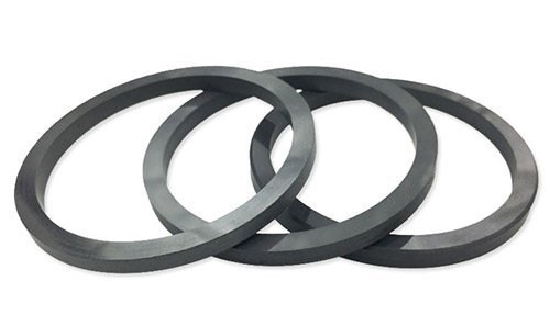
Conductive silicon, as a commonly used focusing ring material, has a conductivity almost similar to that of silicon wafers. However, its disadvantage is poor corrosion resistance in fluorinated plasma. After a period of use, the material of etching machine components often exhibits severe corrosion, seriously reducing its production efficiency. Silicon carbide has similar electrical conductivity and good ion resistance to silicon. The sub etching performance is suitable for focusing ring materials. Usually, the focusing ring is formed by depositing the silicon carbide generated by chemical reactions into a certain shape through vapor deposition, and then mechanically processing the silicon carbide into a focusing ring according to specific usage conditions.
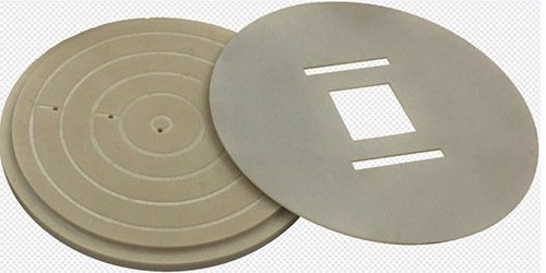
3. Electrostatic chuck (ESC)
During the entire etching process of the chip, it is adsorbed and fixed by the electrostatic chuck (ESC) in the lower electrode system, and RF is introduced to the electrostatic chuck, which forms a DC bias (DC bias) on the chip.This facilitates the etching reaction of plasma on the chip. At the same time, the electrostatic chuck will achieve temperature control on the chip to promote the uniformity of chip etching. The interior of the electrostatic chuck mainly consists of a dielectric layer, a base, and a heating layer. Aluminum oxide and aluminum nitride are commonly used as dielectric layer materials in the production of electrostatic chucks due to their high thermal conductivity and low coefficient of thermal expansion.
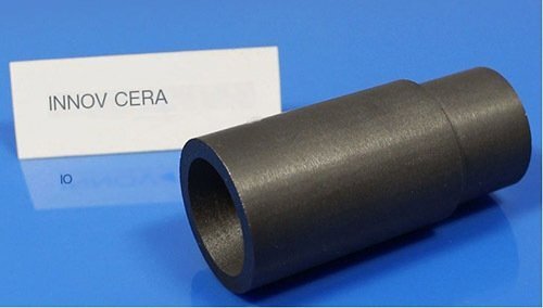
4. Nozzles
The nozzle is used for precise gas flow rate and uniform control to evenly disperse gas into the etching process chamber. These components require high plasma resistance, dielectric strength, and strong corrosion resistance to process gases and by-products. The commonly used ceramic materials include aluminum nitride ceramics and aluminum oxide ceramics. At present, ceramic 3D printing technology can also be used to produce ceramic nozzles in the etching chamber, improving product manufacturing efficiency and usage stability.